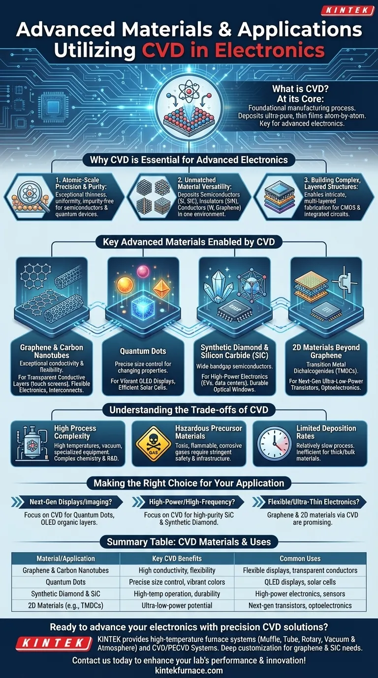
At its core, Chemical Vapor Deposition (CVD) is the foundational manufacturing process enabling the most advanced materials used in modern electronics. It is the go-to technique for depositing ultra-pure, thin films of materials like graphene, carbon nanotubes, quantum dots, and synthetic diamond, which are essential for creating flexible displays, next-generation transistors, and high-performance computing components.
The true significance of CVD in electronics is not just its ability to create novel materials, but its atomic-level precision. This control allows engineers to design and build materials with specific, tailored electronic properties, moving beyond the limits of conventional silicon.
Why CVD is Essential for Advanced Electronics
The move toward smaller, faster, and more powerful electronic devices demands a level of manufacturing control that only processes like CVD can provide. Its utility stems from a few key principles.
Atomic-Scale Precision and Purity
CVD builds materials by depositing one layer of atoms at a time. This results in films that are exceptionally thin, uniform, and free from the impurities that can degrade electronic performance.
For advanced semiconductors and quantum devices, this structural perfection is not a luxury—it is a fundamental requirement for the device to function as designed.
Unmatched Material Versatility
CVD is not limited to a single type of material. It is a flexible technique capable of depositing a vast range of materials critical for building complex electronic devices.
This includes semiconductors like silicon (Si) and silicon carbide (SiC), insulators like silicon nitride, and conductors like tungsten and graphene, all within the same manufacturing environment.
Building Complex, Layered Structures
Modern electronic components, such as CMOS processors, are intricate, three-dimensional structures built from dozens of stacked material layers.
CVD's ability to precisely deposit different materials in sequence is what makes the fabrication of these complex, integrated circuits possible.
Key Advanced Materials Enabled by CVD
CVD is the gateway to producing a new generation of materials whose unique properties are unlocking novel electronic applications.
Carbon-Based Materials: Graphene and Carbon Nanotubes
Graphene is a single layer of carbon atoms with exceptional conductivity and mechanical flexibility. CVD is the primary method for producing large-area, high-quality graphene films.
These films are critical for developing transparent conductive layers for touch screens, flexible electronics, and potentially as a successor to copper interconnects in microchips. Carbon nanotubes offer similar benefits for strengthening composites and improving conductivity.
Quantum Dots
Quantum dots are semiconductor nanocrystals whose electronic and optical properties change with their size. CVD provides the precise control needed to synthesize these particles for specific applications.
In electronics, they are used to create the vibrant, power-efficient colors in high-end QLED displays and to improve the efficiency of photovoltaic solar cells.
Synthetic Diamond and Silicon Carbide (SiC)
Both diamond and SiC are wide-bandgap semiconductors, meaning they can operate at much higher voltages, temperatures, and frequencies than traditional silicon.
CVD is used to grow high-purity films of these materials for high-power electronics in electric vehicles and data centers, as well as durable optical windows for sensors and lasers.
2D Materials Beyond Graphene
CVD is also used to synthesize other two-dimensional (2D) materials, such as transition metal dichalcogenides (TMDCs).
These materials are being heavily researched for creating next-generation, ultra-low-power transistors and other optoelectronic devices, pushing the boundaries of Moore's Law.
Understanding the Trade-offs of CVD
While powerful, CVD is a highly specialized process with inherent challenges that make it unsuitable for every application. Understanding its limitations is key to using it effectively.
High Process Complexity
CVD processes often require high temperatures and high-vacuum conditions, which necessitates sophisticated and expensive equipment.
The chemistry involved is complex, and achieving a stable, repeatable process for a new material can require significant research and development effort.
Hazardous Precursor Materials
The "vapor" in Chemical Vapor Deposition comes from precursor gases, many of which can be toxic, flammable, or corrosive.
Managing these materials requires stringent safety protocols and infrastructure, adding to the operational cost and complexity.
Limited Deposition Rates
Because CVD is designed for precision, it can be a relatively slow process. It excels at creating high-quality thin films but is generally inefficient for producing thick or bulk materials.
For applications requiring thick coatings or large structural parts, other manufacturing methods are often more practical and cost-effective.
Making the Right Choice for Your Application
Selecting the right material and process depends entirely on the performance goals of your electronic device.
- If your primary focus is next-generation displays or imaging: Investigate CVD processes for synthesizing quantum dots and depositing the organic layers used in OLEDs.
- If your primary focus is high-power or high-frequency electronics: Focus on CVD for creating high-purity films of silicon carbide (SiC) and synthetic diamond.
- If your primary focus is flexible, transparent, or ultra-thin electronics: Graphene and other 2D materials synthesized via CVD are the most promising path forward.
Mastering the precise control offered by CVD is fundamental to engineering the future of electronic devices.
Summary Table:
| Material/Application | Key CVD Benefits | Common Uses |
|---|---|---|
| Graphene & Carbon Nanotubes | High conductivity, flexibility | Flexible displays, transparent conductors |
| Quantum Dots | Precise size control, vibrant colors | QLED displays, solar cells |
| Synthetic Diamond & SiC | High-temperature operation, durability | High-power electronics, sensors |
| 2D Materials (e.g., TMDCs) | Ultra-low-power potential | Next-gen transistors, optoelectronics |
Ready to advance your electronics with precision CVD solutions? KINTEK leverages exceptional R&D and in-house manufacturing to provide high-temperature furnace systems like Muffle, Tube, Rotary, Vacuum & Atmosphere Furnaces, and CVD/PECVD Systems. Our deep customization capabilities ensure we meet your unique experimental needs for materials like graphene and SiC. Contact us today to discuss how we can enhance your lab's performance and innovation!
시각적 가이드
관련 제품
- 맞춤형 다목적 CVD 튜브 용광로 화학 기상 증착 CVD 장비 기계
- 진공 스테이션 CVD 기계가 있는 스플릿 챔버 CVD 튜브 퍼니스
- 화학 기상 증착 장비용 다중 가열 구역 CVD 튜브 용광로 기계
- 액체 기화기 포함 슬라이드 PECVD 튜브 가열로 PECVD 장비
- 제어 불활성 질소 수소 대기 용광로


